
In order to safeguard the copper traces and avoid solder bridges during the assembly process, a PCB solder mask is a polymer covering that is put to the surface of the PCB. The solder mask serves as a barrier to stop solder from flowing onto regions where it is not intended to go and is normally put after the copper traces have been etched onto the board.
Small drill holes in the PCB, sometimes called vias, enable for the electrical connection between layers of the board. To create a conductive conduit between the layers of the board, vias are often coated with metal.Through-hole vias cut through the entire board, blind vias only link up specific layers, and buried vias link up layers that are hidden beneath the surface of the board.
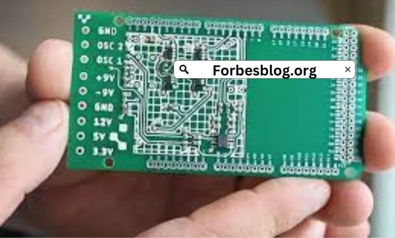
PCB assembly and design depend heavily on the solder mask and PCB holes. The finished PCBs electrical performance and dependability depend on the accurate placement, size, and application of the solder mask.
The following are some creative solutions to PCB hole and solder mask problems:
-
Additive Manufacturing:
Using 3D printing technology to build PCBs in an additive manner is a creative way to address PCB hole concerns. This makes it possible to put holes precisely and to produce intricate designs that would be challenging to make using conventional production techniques.
-
Laser Ablation:
Laser ablation is a cutting-edge method for eliminating specific solder masks from a PCB. In this method, the mask is selectively removed using a laser, exposing the copper underneath. This can be used to redesign a board that has already been put together or to create fine-pitch circuits.
-
Dry Film Solder Mask:
This ground-breaking technique gives you perfect control over the quantity and placement of solder masks on a PCB. Applying a dry solder mask coating on the board and curing it with UV light are the steps in this process. Using a laser ablation process, this produces a precise, homogeneous layer of solder mask that is simple to remove.
-
Automated Inspection:
Automated inspection is a cutting-edge solution to pcb hole and pcb solder mask problems. Manufacturing companies can rapidly and precisely identify flaws in the solder mask application or hole placement by employing computer vision systems and machine learning techniques. This lessens the need for manual examination and can greatly enhance the final product’s quality.
-
Nanocoatings:
An inventive way to shield PCBs from corrosion and environmental harm is with nanocoatings. The board can be shielded against moisture, dust, and other contaminants by manufacturers by coating it with a tiny layer of nanocoating. By doing this, the PCBs lifespan can be greatly extended and less expensive repairs may be required.
-
In-Mould Electronics:
A revolutionary manufacturing method known as in-mould electronics enables the development of fully integrated electronic systems within a single moulded item. This method eliminates the need for separate PCBs and lowers overall production costs by embedding electronics directly into the plastic or resin of a moulded object.
Choosing the Correct PCB Hole Size While Choosing to Maximise Efficiency;
The appropriate hole size can significantly affect the effectiveness of a printed circuit board (PCB) when it comes to design. Even while choosing the right hole size might seem like a minor consideration, it can have an impact on the board’s electrical performance, cost, and ease of manufacture. In this piece, we’ll look at different strategies for selecting the ideal pcb holes size while maximising efficiency.
Understanding the Hole’s Purpose is the First stage in Hole Size Selection Understanding the Hole’s Purpose is the first stage in hole size selection. Is it a via or a through-hole? Vias are used to connect several layers of the board together, whereas through-holes are utilised to transmit a component or a cable through the board.
-
It’s crucial to take the size of the component or lead diameter of the wire that will be flowing through it into account when choosing a through-hole size. A hole that is too small can make assembly challenging and perhaps endanger the board. However, a hole that is too big can lead to a loose fit and a bad electrical connection.
-
Determining the proper hole size also depends on the PCB’s thickness. For the component or wire to pass through the board easily, a thicker board will need a larger hole size. A thinner board, on the other hand, can get away with a smaller hole size because it doesn’t need to hold as much material.
-
Remember the Manufacturing Process: The choice of hole size can also be influenced by the manufacturing process. Although larger holes are typically simpler to drill, plating and filling them may take more time and effort. On the other side, drilling small holes might be more difficult and call for more precise tools. It’s critical to speak with your manufacturer to ascertain the most practical hole sizes for your design.
These pointers will help you choose the right hole size for your PCB design while maximising effectiveness and reducing potential problems.
The Role of pcb Solder Mask in Assembly and Manufacturing;
A thin layer of polymer, usually green in colour, called a solder mask is put to the surface of a printed circuit board (PCB) to assist shield the copper traces and pads from outside influences and unintended solder connections during assembly and production. The solder mask plays a number of significant roles during the production and assembly processes, including:
-
Preventing Solder Bridges: During the assembly process, one of the solder mask’s main purposes is to stop solder bridges from forming between nearby copper traces and pads. Solder can easily flow across adjacent pads or traces without the solder mask, leading to electrical shorts and failures.
-
Environmental Protection: The solder mask aids in shielding moisture, dust, and other environmental aggressors from copper traces and pads. The long-term dependability of the PCB depends on this protection.
-
Enhancing Solderability: By ensuring that the solder only adheres to the intended pads and traces, the solder mask can also enhance the board’s ability to be soldered. This lessens the possibility of solder splatters or balls developing on the board, which may result in electrical shorts or other issues.
The solder mask can also aid in streamlining the production process by giving a visual cue as to where the components should be positioned on the board. By doing this, the chance of mismatched or misplaced components during assembly can be decreased.
Conclusion;
In conclusion, the efficiency, performance, and producibility of electronic devices are significantly influenced by the printed circuit board (PCB) solder mask and hole sizes. The dependability, use, and lifetime of the PCB can be ensured by selecting the proper hole size and using solder mask. While the solder mask shields against environmental influences, prevents solder bridges, increases solderability, streamlines the manufacturing process, and improves aesthetics, the hole size should be set based on the component size, lead diameter, PCB thickness, and manufacturing method. Any PCB design’s success and the application for which it is intended depend on the proper consideration and use of these factors.